Part 2: Boot and blink
In previous post we prepared a custom Rust toolchain for targeting the RV32EC instruction set architecture. We've gone far, but there are still things to be done. Just emitting the correct instruction bytes is not enough, the code has to also do correct things. That is, initialize the processor core and interface with the hardware correctly.
In order to have our code launch on chip boot, there is a bit of house keeping to be done. Turns out fn main is not the first thing that executes in your program. Before any user code can run, a number of house keeping tasks need to be performed. Registers may need to be reset, the .bss and .data sections need to be initialized, stack needs to be setup and some constructors run. We also need definitions for where the linker will actually place our code and data. These duties are filled by runtime (RT) crates in the Rust ecosystem. Since our CH32V003 part is a RISC-V part, we will be using the appropriate riscv-rt crate.
Because we can't use a regular Rust main, let's use the #[entry] attribute from riscv-rt to denote the entrypoint for our program. Note how we must use -> ! for our main function; On bare metal there are no applications, so exiting the application is not really a valid concept. Instead we will enter an infinite loop at the end of our program.
#![no_std]
#![no_main]

use riscv_rt::entry;

#[entry]
fn main() -> ! {
    loop {}
}
We of course need to add the dependency to our Cargo.toml before we can attempt compilation.
$ cargo add riscv-rt
$ cargo build
   ...
   Compiling riscv-rt v0.11.0
error: failed to run custom build command for `riscv-rt v0.11.0`

Caused by:
  process didn't exit successfully: `~/hello-wch/target/debug/build/riscv-rt-c8cb12ace52547c5/build-script-build` (exit code: 101)
  --- stderr
  thread 'main' panicked at 'called `Result::unwrap()` on an `Err` value: Os { code: 2, kind: NotFound, message: "The system cannot find the file specified." }', C:/Users/Aarop/.cargo/registry/src/index.crates.io-6f17d22bba15001f/riscv-rt-0.11.0/build.rs:25:68
As you might have noticed, crates aren't really aware of RV32E yet. The riscv-rt runtime crate is no different. If you peek into the build script, you'll notice it panics when trying to copy a native library [riscv-rt]/bin/riscv32ec-unknown-none-elf.a. These libraries come directly as part of the crate and define the startup routines for RISC-V. These are the very first instructions the processor executes after it receives power, and must be hand written in low level assembly As you might notice, these manually built variants are not the most flexible way about achieving this. There is a draft pull request open for switching to inline assembly, but it's not quite there yet. Besides, we do need quite a different assembly anyways for our 16 register RV32E.
9names has done the heavy lifting on this part, rewriting the startup assembly and building it with our custom LLVM tooling. We can use this work by patching the riscv-rt crate with their fork.
# Cargo.toml
[patch.crates-io]
riscv-rt = { git = "https://github.com/9names/riscv-rt", branch = "rv32e" }
The actual assembly is not very long and the there isn't much difference between the regular startup code and the forked E-aware assembly. It declares our real entry point called _start which stores 0's to all of the registers. Then it loads sp with the address of our stack space and jumps to start of our rust code, _start_rust.
$ cargo build
   ...
   Compiling hello-wch v0.1.0 (~/hello-wch)
   Compiling riscv-rt v0.11.0 (https://github.com/9names/riscv-rt?branch=rv32e#963b8965)
error: linking with `rust-lld` failed: exit code: 1
  |
  = note: rust-lld: error: undefined symbol: _mp_hook
          >>> referenced by lib.rs:411 (src/lib.rs:411)

          rust-lld: error: undefined symbol: _setup_interrupts
          rust-lld: error: undefined symbol: __pre_init
          rust-lld: error: undefined symbol: _sbss
          rust-lld: error: undefined symbol: _ebss
          rust-lld: error: undefined symbol: _sdata
          ...
Now our build is stopped by a bunch of undefined symbols. While the runtime crate provides us with most of the linker scripts needed, we still have to specify where to actually place all the sections in the final image. Otherwise all the sections and their symbols will stay undefined.
Create a file in the crate root called memory.x. This file will define regions of memory on our hardware, and what sections to place into which memory. The CH32V003 contains 2 kilobytes of static RAM and 16 kilobytes of Flash memory.
If we visit the CH32V003 datasheet for more details, we can find the memory map in section 1.2. There are fairly detailed descriptions for each address range, but we are interested in only a few.
| Start address | Size | Description |
|---|---|---|
0x0000_0000 | 128M | Aliased to either Flash or RAM |
0x0800_0000 | 16K | Program flash |
0x1FFF_F000 | 2K | System flash (bootloader) |
0x2000_0000 | 2K | Static RAM |
0x4000_0000 | 256M | Peripheral access |
Depending on the system state, the first address range is mapped to either the flash memory or the random access memory. This is used by debuggers, allowing you to execute and modify code in memory, instead of flashing new firmware constantly. The real flashed code lives at 0x0800_0000 and the real RAM lives at 0x2000_0000. Now that we know where the flash and RAM are, we can fill in our linker script.
PROVIDE(_hart_stack_size = 1K);

MEMORY
{
	FLASH (rx) : ORIGIN = 0x00000000, LENGTH = 16K
	RAM (xrw)  : ORIGIN = 0x20000000, LENGTH = 2K
}

REGION_ALIAS("REGION_TEXT", FLASH);
REGION_ALIAS("REGION_RODATA", FLASH);
REGION_ALIAS("REGION_DATA", RAM);
REGION_ALIAS("REGION_BSS", RAM);
REGION_ALIAS("REGION_HEAP", RAM);
REGION_ALIAS("REGION_STACK", RAM);
Unsurprisingly, we place our read-only data into the read-only flash memory, and the rest goes in into the SRAM. Right at the top we configure our stack size to be 1K. By default riscv-rt uses a stack size of 2K, which would take up our whole memory! As you develop your application, you probably need to tweak this value to fit your needs. (Sidenote, hart is RISC-V lingo for Hardware Thread. Not particularily important for our chip however).
Now that we have a linker script, let's tell Rust to include it in our linking process. This can be done a Rust build script by printing out special commands that Cargo will pick up.
fn main() {
    // Tell rustc to pass linker scripts to LLD
    println!("cargo:rustc-link-arg=-Tmemory.x");
    println!("cargo:rustc-link-arg=-Tlink.x");

    // Rerun this script only when necesary
    println!("cargo:rerun-if-changed=memory.x");
    println!("cargo:rerun-if-changed=build.rs");
}
First two lines tell Cargo to tell rustc to tell the linker to use two linker scripts, memory.x and link.x. We provide the former, and the latter actually comes from the riscv-rt crate.
We can try building it again, but now we run to another error: Our code does not fit in the Flash region! As it turns out, debug builds don't get any real size optimizations or dead code elimination, so fitting even an empty crate into 16K is not possible.
$ cargo build
error: linking with `rust-lld` failed: exit code: 1
  = note: rust-lld: error: section '.text' will not fit in region 'FLASH': overflowed by 12 bytes
          rust-lld: error: section '.text' will not fit in region 'FLASH': overflowed by 158 bytes
          rust-lld: error: section '.text' will not fit in region 'FLASH': overflowed by 190 bytes
          ...
Our options are either building in release mode, or setting the optimization higher for debug builds as well. Since 16K is very little memory, I will choose to change our debug optimization level to "s", meaning LLVM will optimise for binary size. This is done in the Cargo.toml
[profile.dev]
opt-level = "s"
With this change our binary ends up being much much smaller. But what has introducing riscv-rt really changed? Well if you used objdump on the binaries we previously built, you might've noticed they didn't actually contain anything executable.
$ cargo build
   ...
   Compiling hello-wch v0.1.0 (~/hello-wch)
    Finished dev [optimized + debuginfo] target(s) in 22.12s
$ llvm-objdump target/riscv32ec-unknown-none-elf/debug/hello-wch -h
# Before riscv-rt
Sections:
Idx Name              Size     VMA      Type
  0                   00000000 00000000
  1 .riscv.attributes 00000021 00000000
  2 .comment          00000013 00000000
  3 .symtab           00000030 00000000
  4 .shstrtab         00000036 00000000
  5 .strtab           00000034 00000000
# After riscv-rt
Sections:
Idx Name              Size     VMA      Type
  0                   00000000 00000000
  1 .text.dummy       00000000 00000000 BSS
  2 .text             00000284 00000000 TEXT
  3 .rodata           00000030 00000284 DATA
  4 .data             00000000 20000000 DATA
  5 .bss              00000000 20000000 BSS
  6 .heap             00000000 20000000 BSS
  7 .stack            00000800 20000000 BSS
  8 .eh_frame         00000030 00000000
  9 .riscv.attributes 00000021 00000000
  ...
Now we are getting somewhere. If you disassemble the start of the binary, you see riscv-rt has prepared us a nice entry point and some reset, exception and interrupt vectors. Starting at 0x0000_0000 you'll find code that resets all the registers on boot or system fault. There is also a bit called _start_rust that sets up the stack and Rust runtime for us. (Yes, Rust has a runtime, just like C). Lastly, you can find our beloved main section somewhere.
00000184 <main>:
     184: 01 a0         j       0x184 <main>
Short and sweet. The compiler has generated a compressed (16 bit, 2 byte) jump instruction that simply jumps back to itself, realising our infinite loop. We could flash the code to a real CH32V003 now. However, code that does nothing is not particularily useful, nor is it too easy to verify things are working correctly. How about we implement our first embedded project?
Blinken lights
Probably the simplest first thing you can do on a new board is to blink an LED. All you need is access to the GPIO driver and optionally a timer. In a pinch you can just loop in place to cause a delay, so it's really easy to get started.
To drive a blinking LED we need to configure some of the IO pins as an output and toggle it on and off. Our CH32V003 chip has 3 different GPIO banks, each controlling 8 pins. Interestingly enough, these are called the GPIOA, GPIOC and GPIOD. It seems that GPIOB got lost somewhere along the way, but for now we will just need one bank. To figure out how to control these pins, we need to look at the CH32V003's datasheet.
Going back to section 1.2, the memory map, we can see an address range from 0x4001_1000 to 0x4001_1400 called PORT C. We will use GPIOC for our demo, so this is what we are interested in. The GPIO (and all other peripherals) are controlled by writing and reading from these special memory addresses, called control registers. There are many of these control registers. Even a fairly bare bones microcontroller like ours has hundreds of control registers. How do we know what memory address maps to which register?
Register definitions
In addition to the higher level datasheet, there is also the CH32V003 reference manual. This document describes the hardware on much lower level. The current revision (v1.3) is a 181 page PDF, so there is quite a bit to read through. If we scroll through to section 7.3.1, we find the GPIO register description. This table lists the memory addresses of all our relevant GPIO registers. Here are all the entries related to GPIOC:
| Address | Name | Description |
|---|---|---|
0x4001_1000 | R32_GPIOC_CFGLR | Configuration register low |
0x4001_1008 | R32_GPIOC_INDR | Input data register |
0x4001_100C | R32_GPIOC_OUTDR | Output data register |
0x4001_1010 | R32_GPIOC_BSHR | Set/reset register |
0x4001_1014 | R32_GPIOC_BCR | Reset register |
0x4001_1018 | R32_GPIOC_LCKR | Configuration log register |
If you are sharp eyed, you might've noticed that there is only a mention of a "Configuration register low", but no "high". Even more so, each of these 32 bit registers have contiguous addresses, except right after the CFGLR. Manufactures often use different variants of the same architecture for different parts. Let's look up the reference manual for a higher end chip from WCH, like the CH32V208. This part has tons of more features, like Ethernet and USB. Looking into it's GPIO register listing, we do indeed find CFGHR, a "Configuration register high". More so, we not only find our missing GPIOB bank but also a new, fifth GPIOE bank. It seems that in order reduce costs, WCH has chosen to remove 2 banks from the CH32V003's silicion die and reduce the number of pins per bank from 16 to 8. Mystery solved.
So, back to blinking LEDs. To toggle our pin high and low, we need to first configure it into an output pin and then write the data. A bit lower down in the reference manual we find descriptions for each individual register.
7.3.1.1 R32_GPIOC_CFGLR
The 32bit configuration register is split into eight 4 bit sections, each mapping to its respective pin the bank. The 4 bits are further split into a low and high halves, MODE and CNF respectively.
MODE sets which mode the pin operates in. There are 4 possible settings:
| Value | Description |
|---|---|
0b00 | Input mode (default) |
0b01 | Output mode, 10Mhz |
0b10 | Output mode, 2Mhz |
0b11 | Output mode, 50Mhz |
The frequency refers to the maximum switching speed for that mode. Do not ask me what the tradeoffs are for choosing 50Mhz vs 2Mhz, I have not found an answer in the reference manual. By default the chip is set to mode 0b00, the input mode. For our use, we can set the mode to 0b01, aka 10Mhz output.
CNF bits have different meanings depending on what MODE is active.
MODE | Value | Description |
|---|---|---|
| Input | 0b00 | Analog input |
| Input | 0b01 | Floating input |
| Input | 0b10 | Push-pull input |
| Output | 0b00 | Push-pull output |
| Output | 0b01 | Open drain output |
| Output | 0b10 | Multiplexed push-pull output |
| Output | 0b11 | Multiplexed open drain output |
Push-pull is a mode where the pin is connected to either the power or ground rails through internal resistors. For example, to read button state you would use a pull-up input mode and connect the other terminal of the switch to GND. When the switch is not pressed, the internal resistor brings the pin voltage to high. When the switch is activated, the charge is drained to ground and the chip can sense a low value on the pin. When the switch is released again, the pin gets pulled back up.
Open drain instead means that the pin is directly connected to either the power or ground rail.
Multiplexed allow you to connect other peripherals (like serial UART) to your physical pins. For our LED blinking code we will use the push-pull output, so CNF = 0b00.
7.3.1.3 ODR32_GPIOC_OUTDR
Once we have configured our pin as an output, we can start writing values to them. The output data register OUTDR is simply eight 1-bit values corresponding to each of the eight output pins in the bank. Value of 0 means the pin is pulled low, and value of 1 means the pin is pulled high.
Putting it together
Let's write up an LED to our chip. I have designed a very simple breakout board for the SOP8 package variant, the CH32V003J4M6. This package is very minimal, exposing only 6 pins, power and ground. The grid at the center is for a 12-LED charlieplexing circuit, but we can leave those LEDs unsoldered and just use the pins as is.
 Komi is thinking about ferris
The datasheet has pinouts for each of the package variants. When using these low pincount packages the internal chip pins are connected together to expose as much functionality as possible. We have to be careful when choosing what is connected what so that peripherals do not interfere with each other.
Let's connect our LED to pin 5 of the J4M6. This pin has multiple uses, but for us it is connected to GPIOC banks pin 1. This means that we have to configure CFGLR[4..8] (second 4-bit group) with 0b0001 (MODE = 0b01, CNF = 0b00). Then we can write 1 to OUTDR[1]
#![no_std]
#![no_main]

use riscv_rt::entry;
use panic_halt as _;

#[entry]
fn main() -> ! {
    let GPIOC_CFGLR: *mut u32 = 0x4001_1000 as _;
    let GPIOC_OUTDR: *mut u32 = 0x4001_100C as _;

    unsafe {
        // Write 0b0001 to pin 1 configuration
        GPIOC_CFGLR.write_volatile(0b0001_0000);
        // Set pin 1 to high
        GPIOC_OUTDR.write_volatile(0b1_0);
    }

    loop {}
}
Since we are now writing to arbitrary memory locations, we do have to bust out the good 'ol unsafe. Note that we only write to the memory, and never read it back. Normally LLVM would be free to optimise these writes out as dead code, but if we use ptr::write_volatile we tell the compiler that these writes must really happen. LLVM has no understanding of what memory mapped IO is, so we must explicitly tell it to just trust us and keep these memory writes in, even though they look to be useless. We can check the generated assembly again. I've annotated the disassembly with pseudocode of whats happening
00000184 <main>:
     184: 37 15 01 40   lui     a0, 262161       // a0 = (0x0004_0011 << 12)
     188: c1 45         li      a1, 16           // a1 = 0b0001_0000
     18a: 0c c1         sw      a1, 0(a0)        // *(a0 + 0) = a1
     18c: 89 45         li      a1, 2            // a1 = 0b10
     18e: 4c c5         sw      a1, 12(a0)       // *(a0 + 12) = a1
     190: 01 a0         j       0x190 <main+0xc> // loop {}
If you are not familiar with RISC-V assembly, in short what is happening here is we are loading the base memory address of 0x4001_1000 into register a0. This is the register name defined by the ilp32e ABI, so refering back to our table from the previous post we can see that we are really talking about register x10. If you are confused by the constant 262161 (0x4_0011) instead of the full adress, the lui is short for "Load upper immediate". This instruction fills a registers upper 20 bits bit a 20 bit constant, setting the lower 12 bits to zero. It may a little strange, but combined with the offset capability of sw ("Store word") instructions, RISC-V can effectively address the full address space with 32 bit instructions.
As expected, there are 2 stores to our CFGLR and OUTDR. Now let's try it on real hardware. The CH32V003 uses its own single wire debug and flashing protocol for which we need WinChipHead's hardware programmer and its accompanying driver. We connect the SWIO pin of the WCH-LinkE hardware programmer to the pin 5 of the devboard and open WCH-LinkUtility.
The programming tool accepts firmware images in the Intel HEX format. This is a simple flat binary format that is often used for programming microcontrollers. Since LLVM produces an ELF binary, we need to first convert it to HEX before we can flash our chip. For this, our custom LLVM comes in handy again.
$ llvm-objcopy -O ihex target/riscv32ec-unknown-none-elf/debug/hello-wch out.hex
$ cat out.hex
:10000000B700000067808000735040307350403468
:1000100081400141814101428142014381430144C8
:100020008144814601478147970100209381817D6A
...
That sure looks like some Intel HEX. Let's plug it into WCH-LinkUtility and try flashing our chip.
00:17:21:625>> Begin to Erase...
00:17:21:698>> Succeed
00:17:21:702>> Begin to Program and Verify...
00:17:21:903>> Succeed
00:17:21:906>> Begin to Reset...
00:17:21:926>> Succeed
00:17:21:929>> Operation is Successful
However, nothing is happening. The LED still stays off. What have we done wrong? Turns out there is one more register we have to configure. As our world becomes increasingly mobile and battery powered, microcontrollers have naturally adopted advanced power saving features. Since we are only using the C bank of the GPIO peripheral, there is no reason for use to use any microwatts to power banks A or D, or any other peripheral like SPI or I2C.
Like most electronics, our chip is built on Complementary Metal-oxide semiconductor (CMOS) technology. The name comes from the fact that each logical function in the hardware is implemented as two complementary P- and N-type transistors. You do not need to know what those are, but the end result is that CMOS circuits only really consume energy when switching states. To effectively power down a circuit, you just need to stop it. Microcontrollers implement peripheral power management in this manner by clock gating. By disabling the clock signal to a peripheral, nothing in the peripheral circuit can change and thus consume power.
So we turn back to the reference manual and head to chapter 3, Reset and Clock Control. This controller provides you with the ability to fine tune how fast the chip is running and what peripherals are receiving signals. For our demo we can just leave most of it alone and focus on enabling our GPIOC peripheral.
Section 3.3.5.2 details more about controlling peripherals. Interally the RISC-V core and peripherals are connected through few busses, called AHB, APB1 and APB2. These are widely spread standards defined by ARM used in all sorts of embedded devices. The AMBA High-performance Bus (AHB) is generally used for peripherals that require high memory bandwidth, while Advanced Peripheral Bus (APB) is more general purpose. On CH32V003 the AHB is only connected to the chip's SRAM and the DMA engine. Rest of the peripherals are connected to APB1 and APB2. We can find our GPIOC under APB2. After a quick look at the register table, we can spot a promising entry, the RCC_APB2PCENR
The RCC_APB2PCENR (APB2 peripheral clock enable register) is mapped to a memory address of 0x4002_1018 and has one bit for each of the peripherals it controls. Setting the matching bit to 1 enables clocking that peripheral. Our GPIOC is mapped to RCC_APB2PCENR[4], so lets add a line to enable the bit. We also change the infinite loop to set the pin off and on repeatedly. We have not configured any timer peripherals yet, so we will use a busy spin loop to slow down the blinking rate. Using a hint function from core we can ensure that Rust won't optimise the "useless" timing loops away. If we did not loop in place for a million instructions, the LED would flash so fast that we could not even perceive it going dark.
#![no_std]
#![no_main]

use riscv_rt::entry;
use panic_halt as _;

#[entry]
fn main() -> ! {
    let RCC_APB2PCENR: *mut u32 = 0x4002_1018 as _;
    let GPIOC_CFGLR: *mut u32 = 0x4001_1000 as _;
    let GPIOC_OUTDR: *mut u32 = 0x4001_100C as _;

    unsafe {
        // Enable clocks to the GPIOC bank
        RCC_APB2PCENR.write_volatile(0b1_0000);
        // Set pin 1 to output
        GPIOC_CFGLR.write_volatile(0b0001_0000);

        loop {
            // Set pin 1 to high
            GPIOC_OUTDR.write_volatile(0b1_0);

            for _ in 0..1_000_000 {
                core::hint::black_box(()); // Do nothing, but keep the loop
            }

            // Set pin 1 to low
            GPIOC_OUTDR.write_volatile(0b0_0);

            for _ in 0..1_000_000 {
                core::hint::black_box(()); // Do nothing, but keep the loop
            }
        }
    }
}
Rebuild, objcopy, flash. Hit execute and... Tada, our LED is now blinking!
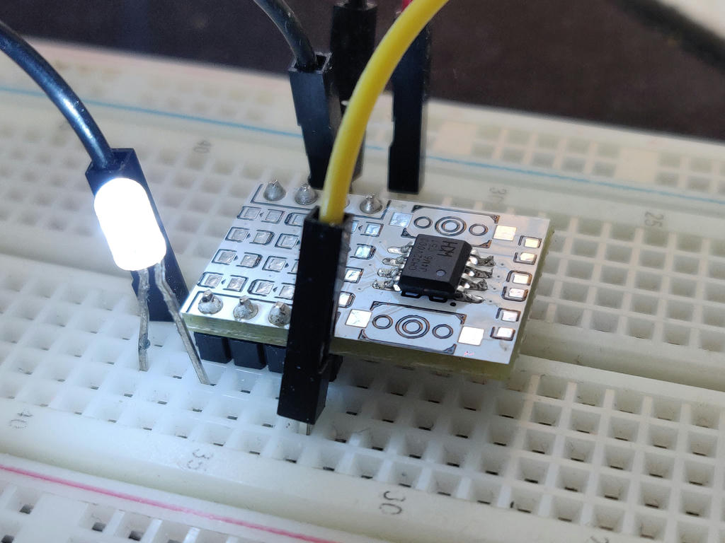 Apply a little imagination and the LED will be blinking away
That sure was a long trip, but the end results are glorious, right? At this point we could declare our porting project complete, having achieved the classic Hello World of embedded. While manually looking up addresses and writing to raw pointers works, it's not very Rusty. In the next post we will look at PACs and the embedded-hal ecosystem.